A holistic integration approach will be critical to success
Overview
The global automotive market is one of today’s most exciting and challenging industry segments, with dynamic waves of innovation and change, including electrification of vehicles, advanced driver assistance systems (ADAS), fully autonomous driving applications, improved safety, reduced pollution, enhanced communications/infotainment systems, and much more!
A key factor for success across all these new transformational applications will be the capability to efficiently interconnect the wide range of sensors, electronic control units (ECUs), actuators, motors, and other elements using robust, customized, and well-integrated interconnector solutions.
This Technical Bulletin provides an overview of the key challenges, with a deeper dive into the design and production considerations for advanced automotive sensor applications. Sensors are one of the challenging areas where a holistic custom interconnector integration approach can be most beneficial.

Fig 1. Multiple Data Streams in Next-Gen Vehicles
Key Elements for Success with Next-Gen Automotive Connectivity
Handling denser, higher speed signaling in new-generation automotive applications requires continual innovation of interconnect design practices. It is also important to “zoom-out” and look at the whole picture to optimize overall integration.
Key factors for success include:
- Optimizing signal interfaces and minimizing signal paths
- Managing thermal issues
- Mitigating noise and EMI/RFI interference
- Using molding and vertical integration strategies
In the following sections, we take a deeper look at how these issues are relevant to the integration of advanced sensors that have become a critical factor for success in automotive applications such as ADAS and ultimately for fully autonomous driving applications.
Optimizing Signal Interfaces and Minimizing Signal Paths
Real-time performance of sensors in automotive applications with minimal latency can be a life-or-death factor in driver-assist and autonomous driving scenarios.
These applications typically incorporate many RADAR and/or LIDAR sensors all around the vehicle to provide a full 360-degree view of the surrounding environment, continuously producing multiple content-rich, real-time data streams that must be quickly processed and communicated to ECUs for on-the-fly decisions.
The challenges for automotive designers to accommodate higher data rates is like what the communications industry went through in transition to 5G telecom as data rates increased from 100Mbps to multi-gigabit bandwidths. Automotive applications of the past rarely had to deal with such high-speed data rates and never faced the challenges of integrating data from many different sensors in real-time – with critical safety results on the line.
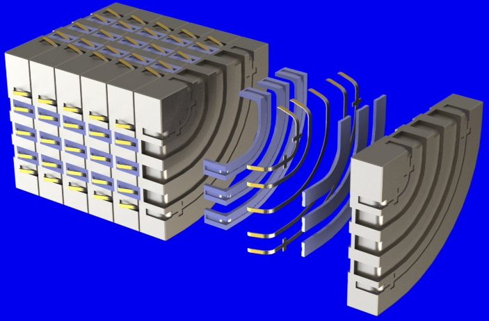
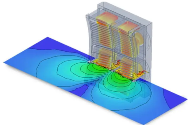
Fig 2. High speed connector design with optimized signal integrity performance
In addition to dealing with higher speeds, sensors in the automotive sector also often must be integrated carefully into the cover to withstand sealing and mechanical force requirements.
The need to optimize signal interfaces and minimize signal paths means that creating effective sensor interfaces for automotive applications can no longer be achieved by simply using off-the-shelf standard components – nor can it be treated as a straightforward build-to-print specification.
These new advanced designs require a holistic and collaborative approach between vehicle manufacturers and connector design partners to create sensor interfaces that are optimized for performance from the initial concept, through prototyping, testing, and full production ramp-up.
Managing Thermal Issues
Higher speeds and tighter functional integration in these new compact sensor module designs are also significantly raising the bar regarding the management of thermal issues.
As with signal optimization, effective thermal management typically also takes a holistic approach that integrates multiple mitigation schemes. In many sensor deployments, the natural airflow from a vehicle moving at highway speeds provides a baseline cooling effect but this is rarely sufficient by itself. Some complex sensors, such as forward-looking cameras, may even embed powered ventilation fans, but such an approach is typically too costly and bulky for most small RADAR or LIDAR sensors, especially given the high number of sensors used in ADAS or fully autonomous applications. Fans also consume a significant amount of electricity and create an additional potential point of failure that is multiplied by a large number of sensors in each vehicle.
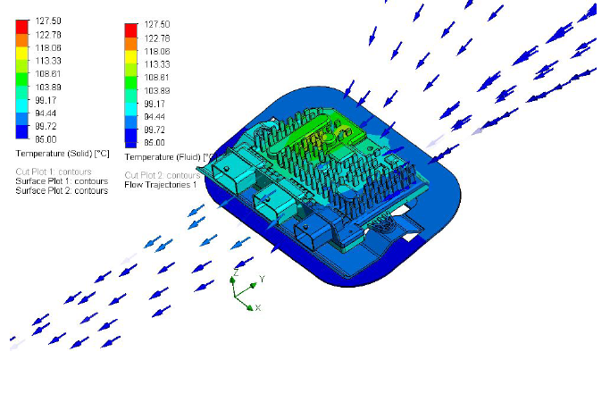
Fig 3. Thermal Management Solution – Embedded Heat Spreader for ADAS Sensor Module
Intelligently integrating advanced passive thermal management techniques provides the best combination of cooling, robust lifecycles, and cost-effectiveness. One such approach is the embedding of heat spreaders in the sensor module packaging. By using a plate or block of material with high thermal conductivity, such as copper or aluminum, a passive heat spreader can continuously remove heat from the module during operation, without the need for an externally powered fan or other active heat management method.
Mitigating Noise and EMI/RFI Interference
Dealing with EMI/RFI interference is also a critical element for success with implementing advanced automotive sensor arrays. Electromagnetic noise is a concern both from the standpoint of external interference with the sensor operation and the need to prevent unwanted interference generated by the module itself.
In helping automotive makers design and integrate effective EMI/RFI shielding over many years of collaboration, ENNOVI has developed a wide range of customizable shielding approaches, materials options, and integration methodologies.

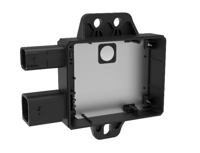
Fig 4. EMI shielding done by Vacuum metallization process
The amount of EMI/RFI reduction depends on the material used, its thickness, the size of the shielded elements, the frequencies to be blocked, as well as the size, shape and orientation of holes in the shield. Regarding materials, traditional shielding effectively uses conductive metals such as copper, brass, nickel, silver, steel or tin. In addition, the movement toward using non-metallic materials is giving rise to shielding made from conductive composites, plastics, etc. ENNOVI is working closely with leading plastic material suppliers to develop and integrate these types of enhanced EMI solutions.
The keys to success once again are rooted in taking a holistic, end-to-end, collaborative approach to the entire design process from concept to final production and involving knowledgeable partners early in the consideration of application-specific design methodologies. Testing and simulation are also important throughout the design process to assure effective EMI performance.
Leveraging Advanced Molding and Vertical Integration Strategies
Perhaps the most important factor for success with designing new-generation sensors with integrated high-performance interconnections is taking a holistic approach to the entire sensor module design and manufacturing techniques. It is also important to work with partners who can provide a range of vertical process integration options.
Molding experience and process capabilities are particularly important for integrated sensor designs because of the need to intelligently combine multiple functional elements and the external communications interface in a single compact, pluggable module.
ENNOVI design teams have found good results with high-temp, glass-filled plastic molding solutions, such as Polyphenylene Sulfide (PPS), Polyphthalamide (PPA), or Polybutylene Terephthalate (PBT), depending on the needs, that can deliver the best combination of thermal characteristics, electrical performance, chemical resistance, and material strength needed for success.
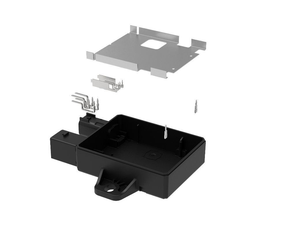
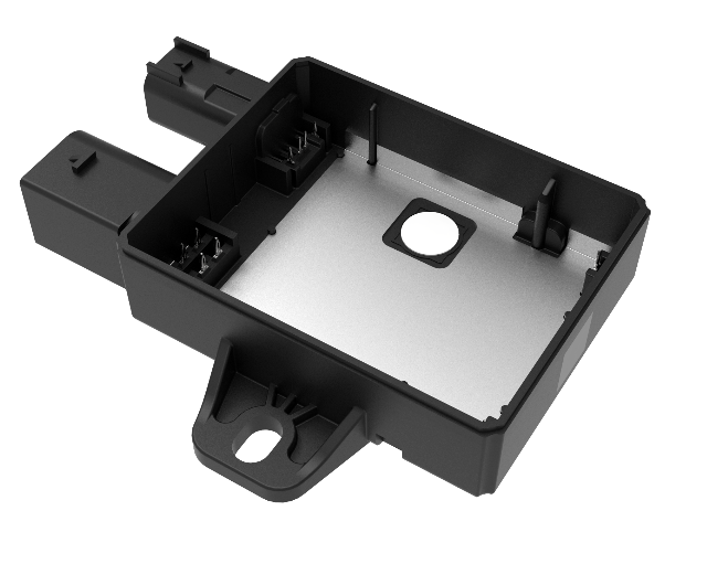
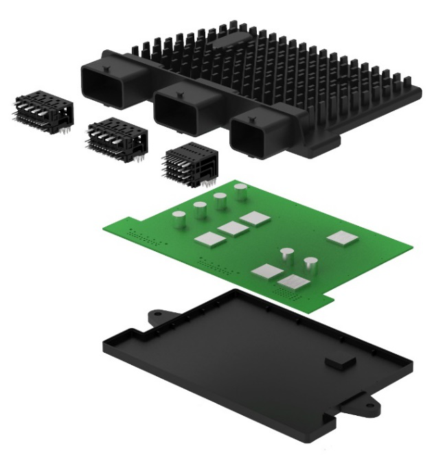
Fig 5. Advance Molding and Vertical Integration
Radar housing done by Insert Molding process
Sequencing of the molding process is another key factor for success to avoid voids in the fill that could degrade thermal conductivity and/or lifecycle robustness. Also, the ability to perform rigorous thermal and finite element analysis can be critical to making the sensor module designs foolproof for high-volume production as required in the automotive industry.
Summary
As described in this Technical Bulletin there is no “one-size-fits-all” approach to optimizing interconnects for next-generation automotive applications, especially with critical sensor designs that enable ADAS or autonomous driving applications.
Therefore, automotive companies need to adopt a holistic, end-to-end approach to creating customized interconnector solutions that integrate seamlessly with their application-specific requirements. To accomplish this, it is important to work closely from the initial concept through production ramp-up with vendors that have a proven track record across all the disciplines described in this Technical Bulletin.
ENNOVI not only has the experience and expertise, but we have also taken the proactive step of creating a broad-based foundation of configurable and adaptable interconnect technologies and vertical integration methodologies for designing and producing custom connector solutions.
These capabilities are backed by the ENNOVI worldwide design, distributed manufacturing and logistics organization that provides unparalleled local support for automotive makers across the globe.
For more information email us at communications@ennovi.com.